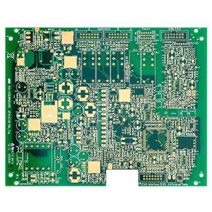
Custom FR4 High Tg 1oz Copper Thickness Multilayer PCB circuit board with ENIG Surface
The basic composition of printed circuit board (PCB)
PCB circuit board (PCB), also known as printed circuit boards, printed circuit board, or PCB, English abbreviation PCB (printed circuit board) or the PWB (printed wiring board), insulation board as base material, cut into a certain size, with at least one conductive graphics, and cloth have a hole (such as component hole, fastening hole, hole metallization, etc.), is used to replace previous device electronic components of the chassis, and realize the connection between the electronic components.Because the board is made by electronic printing, it is called "printed circuit board".The customary term "printed circuit board" is not accurate, because there are no "printed components" on the printed board, only the wiring.
Second, the basic composition
At present, the circuit board is mainly composed of the following:
1. Circuit and Pattern: The circuit is used as a tool to conduct between the original parts. In the design, a large copper surface will be additionally designed as the grounding and power layer.The lines and drawings were made at the same time.
2.Dielectric layer (Dielectric) : used to maintain the insulation between the lines and the layers, also known as the substrate.
3. hole (Through hole/via) : Through hole can make more than two levels of lines Through each other, the larger Through hole is used as part plug-in, in addition to the non-through hole (NPTH) is usually used as a surface mount positioning, fixing screws used during assembly.
4. Solder resistant ink (Solder resistant /Solder Mask) : not all copper surface to eat tin parts, so non-tin eating area, will print a layer of isolation copper surface to eat tin material (usually epoxy resin), to avoid short circuit between non-tin eating tin lines.According to different technology, divided into green oil, red oil, blue oil.
Company Introduction
Abis Circuits Co., Ltd is a professional PCB manufacturer which was established on Oct, 2006 and focus on
double side, Multilayer and HDI pcb mass production.
We have two factories together , the factory in Shenzhen is specialized in small and middle volume orders and the
factory in Huizhou is for big volume and HDI.
Pre-Sale and After-Sale Service
1 Hour quotation
2 hours complaint feedback
7*24 hour technical support
7*24 order service
7*24 hour delivery
7*24 production run
We Can Offer :
1. PCB Manufacture: PCB file or Gerber file needed
2. PCB PCBA SMD SMT Assembly: Gerber File and Bom list needed
3. Reverse Engineering - PCB Copy, PCB Clone, IC Decode
4. Professtional Components Procurement
5. PCB PCBA Finished Product Test
6. PCB And PCBA Mass-Production
Capacity
| | High precision prototype | PCB bulk production |
| Max Layers | 1-28 layers | 1-14 layers |
| MIN Line width(mil) | 3mil | 3mil |
| MIN Line space(mil) | 3mil | 3mil |
| Min via (mechanical drilling) | Board thickness≤1.2mm | 0.15mm | 0.2mm |
| Board thickness≤2.5mm | 0.2mm | 0.3mm |
| Board thickness>2.5mm | Aspect Ration≤13:1 | Aspect Ration≤13:1 |
| Aspect Ration | Aspect Ration≤13:1 | Aspect Ration≤13:1 |
| Board thickness | MAX | 8mm | 7mm |
| MIN | 2 layers:0.2mm;4 layers:0.35mm;6 layers:0.55mm;8 layers:0.7mm;10 layers:0.9mm | 2 layers:0.2mm;4 layers:0.4mm;6 layers:0.6mm;8layers:0.8mm |
| MAX Board size | 610*1200mm | 610*1200mm |
| Max copper thickness | 0.5-6oz | 0.5-6oz |
| Immersion Gold/ Gold Plated Thickness | Immersion Gold:Au,1—8u”
Gold finger:Au,1—150u”
Gold Plated:Au,1—150u”
Nickel Plated:50—500u” | |
| Hole copper thick | 25um 1mil | 25um 1mil |
| Tolerance | Board thickness | Board thickness≤1.0mm:+/-0.1mm
1.0mm<Board thickness≤2.0mm:+/-10%
Board thickness>2.0mm:+/-8% | Board thickness≤1.0mm:+/-0.1mm
1.0mm<Board thickness≤2.0mm:+/-10%
Board thickness>2.0mm:+/-8% |
| Outline Tolerance | ≤100mm:+/-0.1mm
100<≤300mm:+/-0.15mm
>300mm:+/-0.2mm | ≤100mm:+/-0.13mm
100<≤300mm:+/-0.15mm
>300mm:+/-0.2mm |
| Impedance | ±10% | ±10% |
| MIN Solder mask bridge | 0.08mm | 0.10mm |
| Plugging Vias capability | 0.25mm--0.60mm | 0.70mm--1.00mm |
Lead Time
Lead Time
| Category | Quickest Lead Time | Normal Lead Time |
| Double sideds | 24hrs | 120hrs |
| 4 Layers | 48hrs | 172hrs |
| 6 Layers | 72hrs | 192hrs |
| 8 Layers | 96hrs | 212hrs |
| 10 Layers | 120hrs | 268hrs |
| 12 Layers | 120hrs | 280hrs |
| 14 Layers | 144hrs | 292hrs |
| 16-20 Layers | Depends on the specific requirements |
| Above 20 Layers | Depends on the specific requirements |
Quality Control

Certification
Why choose us?
· With ABIS, customers significantly and effectively reduce their global procurement costs. Behind each service provided by ABIS, is hidden a cost saving for customers.
. We have two shop together, one is for prototype, quick turn, small volume making. The other is for mass production also for HDI board, with highly skilled professional employees, for high quality products with competitive price and on-time delivery.
. We provide very professional sales, technical and logistic supports, on a world-wide basis.hours complaint feedback.
FAQ
Q: How about your delivery date ?
A: In general,smaples need 7 working days,mass production need 15-20 working days.
Q: What is your minimum order quantity?
A: NO MOQ.
Q: What is your advandage than other supplier ?
A: We have over 15 years experience in produce PCB services and have reliable of raw material suppliers. We can find out the best source to consistently reduce your cost.
Q: How about your supply capacity?
A: Our supply capacity is around 500000sqm each day.
Q: If No PCB file/Gerber file, only have the PCB sample,could you produce PCB board for me?
A: Yes, we could help you to clone the PCB board . Just send us the sample PCB , then produce for you. The cost depends on the PCB.
Q: Is safty for my PCB design for manufacturing?
A: All customer's copyright will never manufacture PCB board for someone else with your files unless we receive written.
Please keep us informed for any interest!
ABIS cares every your order even 1 piece!