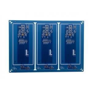
4L 2u'' HDI Printed Circuit Board Blue Solder Mask Immersion Gold With Immersion Gold
Company Profile:
Abis Circuits Co., Ltd is a professional PCB manufacturer in China, Shenzhen. With 14 years+ development, we could make the PCB from 1L to 20L, with a monthly production capability of 60,000 square meters. Abis Circuits is providing high-quality bare PCB and PCB assembly service, including components sourcing, function test, conformal coating, and complete assembly for clients all over the world, Our main market is Europe, north USA, Australia, South America, and Asia.
More than 4 years of working experience for technical backbone, 85% of front-line operation staff, more than 3 years of working experience.
Operation plant space:
(I) 10000 Square meters
(II) 60000 Square meters
Now we have passed ISO9001, ISO14001, UL, etc., With constant hard work of our staff and ongoing support from customers both home and abroad, we can provide up to 20 layers, Blind and buried Board, high-precision(Rogers), High TG, Alu-base and flexible boards to our customer with fast turn and high-quality level.
1. Single, Double side & Multi-layer PCB.
2. Buried/Blind Vias, Via in Pad, Counter Sink Hole, Screw Hole(Counterbore), Press-fit, Half Hole.
3. HASL lead-free, Immersion Gold/ Silver/Tin, OSP, Gold plating/finger, Peelable mask,
4. Printed Circuit Boards adhere to IPC Class 2 & 3 international PCB standard.
5. Quantities range from prototype to medium&big batch production.
6.100% E-Test.
PCB Board Product Description
| Number of layers | 4 – 22 layers standard, 30 layers advanced |
| Technology highlights | Multilayer boards with a higher connection pad density than standard boards, with finer lines/spaces, smaller via holes and capture pads allowing microvias to only penetrate select layers and also be placed in surface pads. |
| HDI builds | 1+N+1, 2+N+2, 3+N+3,4+N+4, any layer in R&D |
| Materials | FR4 standard, FR4 high performance, Halogen free FR4, Rogers |
| Copper weights (finished) | 18μm – 70μm |
| Minimum track and gap | 0.075mm / 0.075mm |
| PCB thickness | 0.40mm – 3.20mm |
| Maxmimum dimensions | 610mm x 450mm; dependant upon laser drilling machine |
| Surface finishes available | OSP, ENIG, Immersion tin, Immersion silver, Electrolytic gold, Gold fingers |
| Minimum mechanical drill | 0.15mm |
| Minimum laser drill | 0.10mm standard, 0.075mm advanced |
PCB Product Detail
| Production capacity of hot-sale products |
| Double Side/Multilayer PCB Workshop | Aluminum PCB Workshop |
| Technical Capability | Technical Capability |
| Raw materials: CEM-1, CEM-3, FR-4(High TG), Rogers, TELFON | Raw materials: Alurminum base, Copper base |
| Layer: 1 layer to 20 Layers | Layer: 1 layer and 2 Layers |
| Min.line width/space: 3mil/3mil(0.075mm/0.075mm) | Min.line width/space: 4mil/4mil(0.1mm/0.1mm) |
| Min.Hole size: 0.1mm(dirilling hole) | Min.Hole size: 12mil(0.3mm) |
| Max. Board size: 1200mm* 600mm | Max.Board size: 1200mm* 560mm(47in* 22in) |
| Finished board thickness: 0.2mm- 6.0mm | Finished board thickness: 0.3~ 5mm |
| Copper foil thickness: 18um~280um(0.5oz~8oz) | Copper foil thickness: 35um~210um(1oz~6oz) |
| NPTH Hole Tolerance: +/-0.075mm, PTH hole Tolerance: +/-0.05mm | Hole position tolerance: +/-0.05mm |
| Outline Tolerance: +/-0.13mm | Routing outline tolerance: +/ 0.15mm; punching outline tolerance:+/ 0.1mm |
| Surface finished: Lead free HASL, immersion gold(ENIG), immersion silver, OSP, gold plating, gold finger, Carbon INK. | Surface finished: Lead free HASL, immersion gold(ENIG), immersion silver, OSP etc |
| Impedance control tolerance: +/-10% | Remain thickness tolerance: +/-0.1mm |
| Production capability: 50,000 s.q.m/month | MC PCB Production capability: 10,000 s.q.m/month |
Lead Time
| Category | Quickest Lead Time | Normal Lead Time |
| Double sideds | 24hrs | 120hrs |
| 4 Layers | 48hrs | 172hrs |
| 6 Layers | 72hrs | 192hrs |
| 8 Layers | 96hrs | 212hrs |
| 10 Layers | 120hrs | 268hrs |
| 12 Layers | 120hrs | 280hrs |
| 14 Layers | 144hrs | 292hrs |
| 16-20 Layers | Depends on the specific requirements |
| Above 20 Layers | Depends on the specific requirements |
PCB Manufacturing Process
- The process starts with designing Layout of the PCB using any PCB designing software / CAD Tool (Proteus, Eagle, Or CAD).
- All rest of the steps are of Manufacturing Process of a Rigid Printed Circuit Board is same as Single Sided PCB or Double Sided PCB or Multi-layer PCB.
Our responsibility:
We know that the PCB is a critical key component for our customers. And we know for sure that anything can happen during the complex production process involved – and it often does. In our world, taking full responsibility means a lot of things, including a responsible and sustainable approach in everything we do – socially, environmentally and ethically. When a problem occurs, we try as hard as we can to understand the problem and find a solution. Our mindset is that we own the problem and don’t leave until we have cleared it up.
FAQ
Q1:Are you a factory or trade company?
-Abis is a PCB/FPC/PCBA manufacturer/factory. We pecialize in PCB/PCBA Board for over 10 years.
Q2: How can I get a quotation:
-Please send gerber file with format: .PCB / .P-CAD / .DXP / .Gerber
Q3: Do you have PCB in stock?
-It depends on. Most of our PCB board are customized, which according to Gerber file.
. ABIS has samples in stock that could be sent to you for quality checking always.
Q4: Will my PCB files be checked?
-Checked within 12 hours. Once Engineer's question and working file be approved, production will start.
Q5: What do you require in order to produce an assembly quotation?
-Bill of materials (BOM) detailing:
a), manufacturers parts numbers,
b), components suppliers' parts number (e.g. Digi-key, Mouser, RS )
c), PCBA sample photos if possible.
d), Quantity
Q6: What's your shipping way ?
A: 1. We have our own forwarder to ship goods by DHL, UPS, FEDEX, TNT,EMS.
2. If you have your own forwarder, we can cooperate with them.
Please keep us informed for any interest!
ABIS cares every your order even 1 piece!