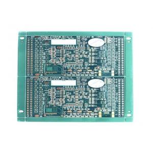
HASL Lead Free Double Layer PCB Rigid circuit board
Brief Introduction
Abis Circuits Co. Ltd, established in 2006, Located in Shenzhen, our company has about 1100 workers and two PCB workshops with about 60,000 square meters.
Product Detail
| 1 | Layers | 2 |
| 2 | Material | FR4 |
| 3 | Board thick | 1.6mm |
| 4 | Cu weight | 1OZ |
| 5 | Min hole | 0.13mm |
| 6 | Usage | Audio |
| 7 | Min line | 0.18mm |
| 8 | Surface coating | HASL lf |
| 9 | Copper wall | 20um |
| 10 | Shape tolerance | ±0.1mm |
| 11 | Solder mask | 25m |
| 12 | PTH | ±0.075mm |
| 13 | Profiling | Rout |
OEM PCB Capacity
| Items | Capability |
| Layer Counts | 1-20layers |
| Material | FR4, High TG FR4, PTFE,Cu base, Rogers, Aluminium base, etc |
| Maximum Size | 600mm x 1200mm |
| Board Outline Tolerance | ±0.10mm |
| Board Thickness | 0.20mm-8.00mm |
| Thickness Tolerance(t≥0.8mm) | ±8% |
| Thickness Tolerance(t<0.8mm) | ±10% |
| Insulation Layer Thickness | 0.075mm-5.00mm |
| Minimum Line | 0.075mm |
| Minimum Space | 0.075mm |
| Out Layer Copper Thickness | 18um-350um |
| Inner Layer Copper Thickness | 17um-175um |
| Drilling Hole(Mechanical) | 0.15mm-6.35mm |
| Finish Hole(Mechanical) | 0.10mm-6.30mm |
| Diameter Tolerance(Mechanical) | 0.05mm |
| Registration(Mechanical) | 0.075mm |
| Aspect Ratio | 16:01 |
| Solder Mask Type | LPI |
| SMT Mini. Solder Mask Width | 0.075mm |
| Mini. Solder Mask Clearance | 0.05mm |
| Plug Hole Diameter | 0.25mm*0.60mm |
| Impedance Control Tolerance | ±10% |
| Surface Finish | HASL, Lead Free HASL, Immersion tin, Immersion gold, Gold plating, Immersion silver, OSP, etc. |
| Soldermask Color | Green, White, Black, Red, Yellow, Blue |
| Silkscreen Color | White, Black, Yellow, Blue |
Lead time
| Board Type | Manufacturing Lead Time |
| Single Sided | 5 – 20 Days dependant on volume |
| PTH | 7 – 25 Days dependant on volume |
| Multilayer | 15 – 30 Days dependant on volume & Technology |
·
| Air Freight Lead Time – 4 Days |
| Sea Freight Lead Time – 30 Days |
| All Far East lead times are subject to customs clearance |
| Premium International shipments can be arranged by DHL, Fedex, UPS or TNT at extra cost |
Product

Related Product
-Common packaging:
- PCB: Sealed bag, Anti-static bags, Suitable carton.
- PCBA: Antistatic foam bags, Anti-static bags, Suitable carton.
- Customized Packaging: The carton outside will be printed the name of the customer address, mark, the customer needs to specify the destination and other information.
Process
FAQ
Q1: What files do you use in PCB fabrication?
A1: Gerber, PCB. Auto CAD
Q2: How do you make sure the quality?
A2: Our Product is all 100% tested including Flying Probe Test (for sample), E-test (mass) or AOI.
Q3: What is your minimum order quantity (MOQ)?
A3: Our MOQ is 1 PCS, sample and mass production all can support.
Q4: Will you keep our information and files secret?
A4: Sure! It is our basic principle to keep business secrets to protect our customers' rights and behalf.
Q5: How to work with you?
A5: -Email and send us the PCB layout file, BOM list
- We will provide reply confirmation within 12 hours and reply to the offer within 3-5 days.
- Waiting for your company to confirm the price, order and payment method.
- We will start the production.
Q6: What service do you have?
A6: We are the factory. We have our PCB manufacturing & Assembly factory.
We can offer a one-stop service from PCB manufacturing to PCB assembling, testing, housing, and other value-added services.